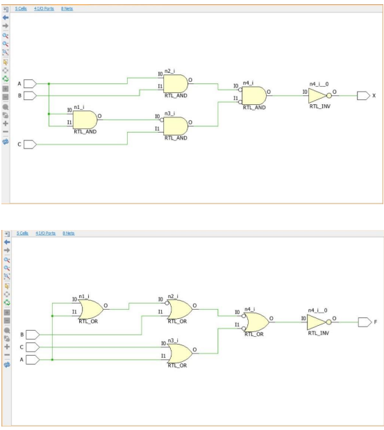
Experiment 1: (Design and Simulation of boolean functions using Verilog HDL. Hardware implementation of a Boolean function in sum of products and product of sums expressions using universal gates.)
RTL Schematic:
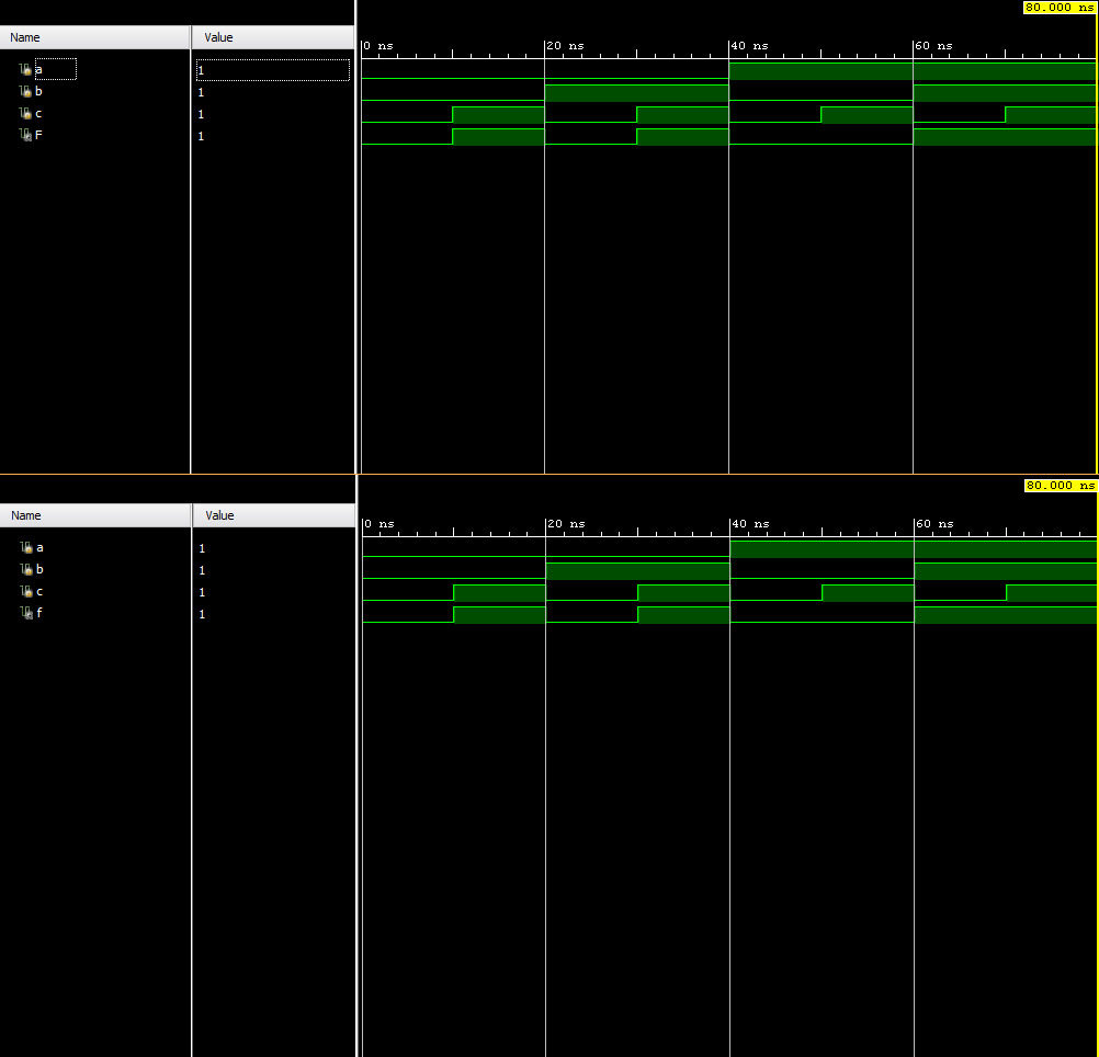
Testbench Simulation:
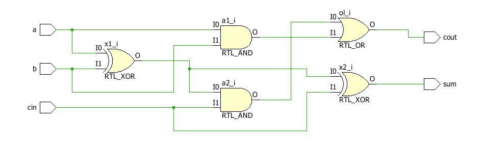
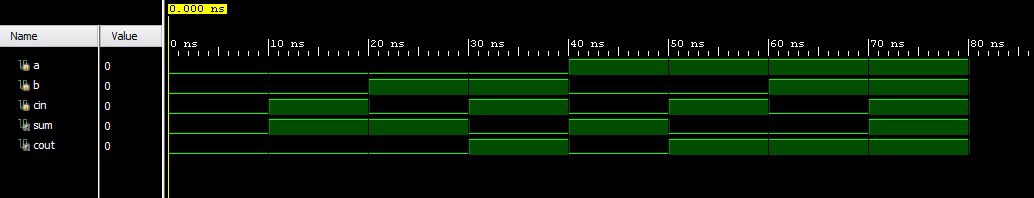
Experiment 2:(Design and Simulation of Full Adder circuit using Verilog HDL. Hardware implementation of Full Adder circuit using logic gates.)
RTL Schematic:
Testbench Simulation:
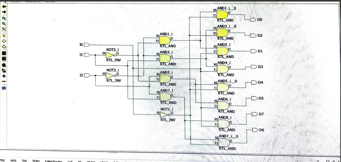
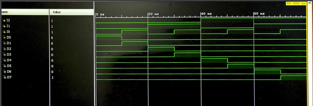
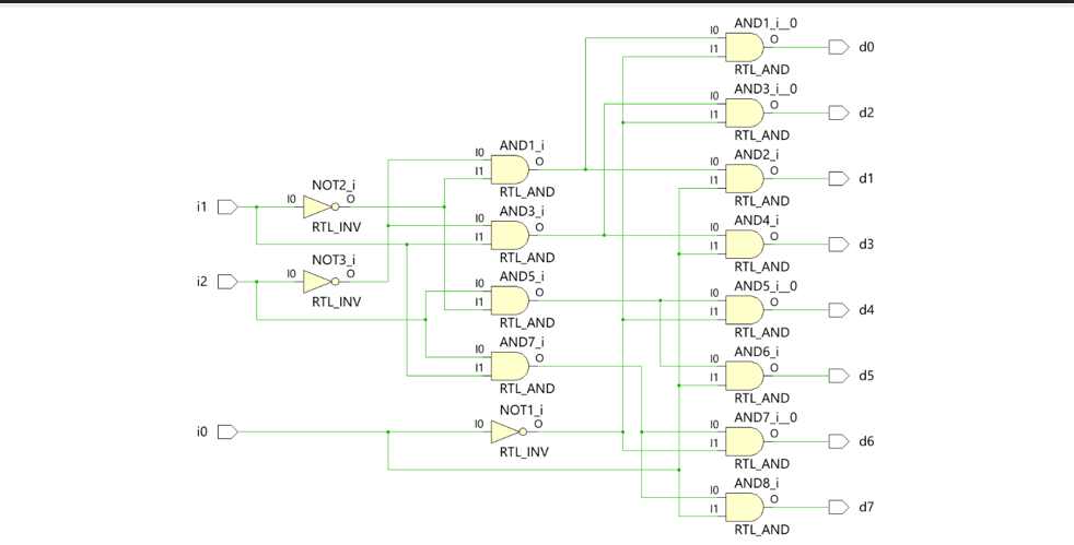
Experiment 3:(Design and Simulation of 3 line to 8 line active high decoder using Verilog HDL.Realization of 3 variable Boolean function using active low decoder)
RTL Schematic:
Testbench Simulation:
Experiment 4:(Design and Simulation of 8-to-1-line Multiplexer using Verilog HDL. Generation of 4 variable logic function using 8-to-1-line Multiplexer)
RTL Schematic:
Testbench Simulation:
Experiment 5:(Design and simulate JK flip-flop and D flip-flop using Verilog behavioral modeling. Designing of JK flip-flop using D flip-flop and 2X1 Multiplexer.)
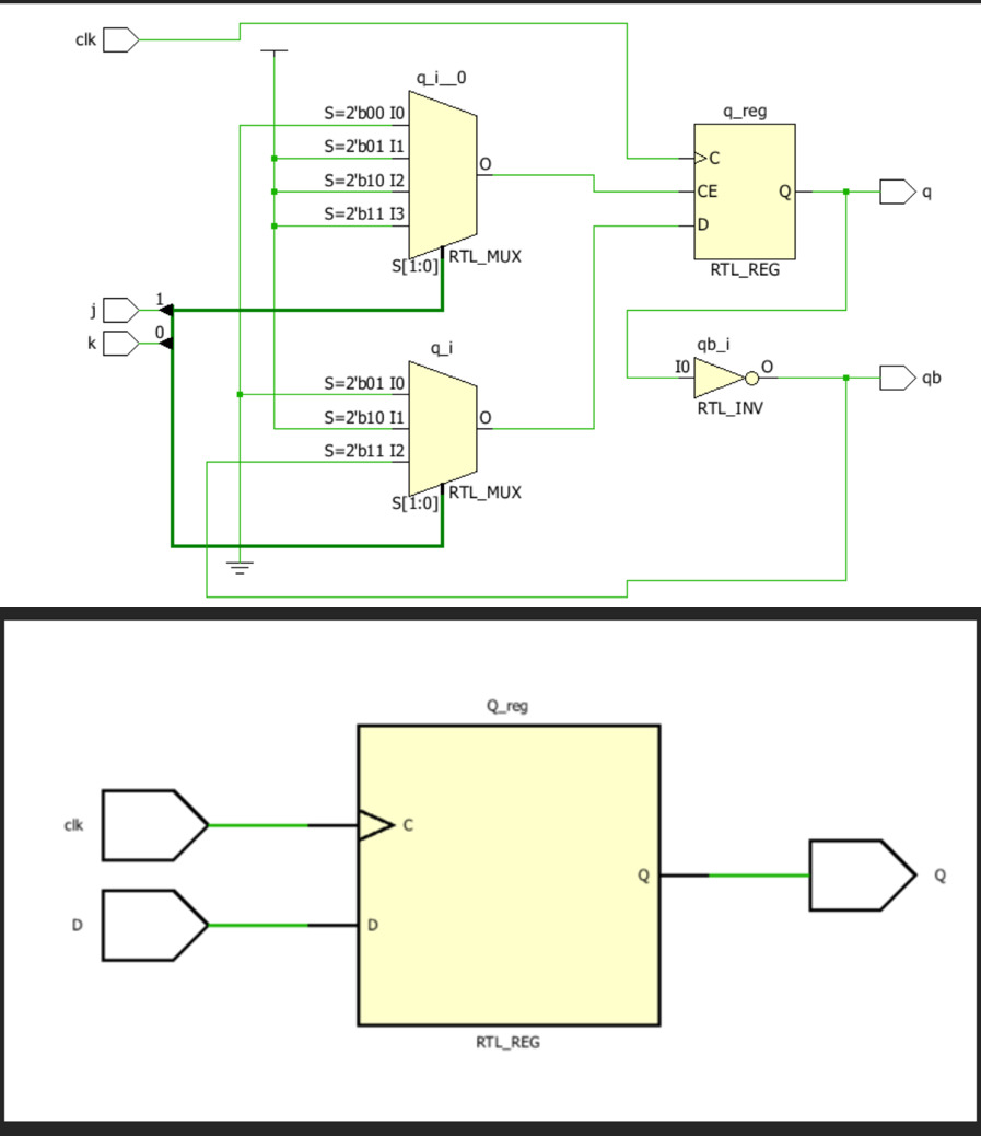
RTL Schematic:
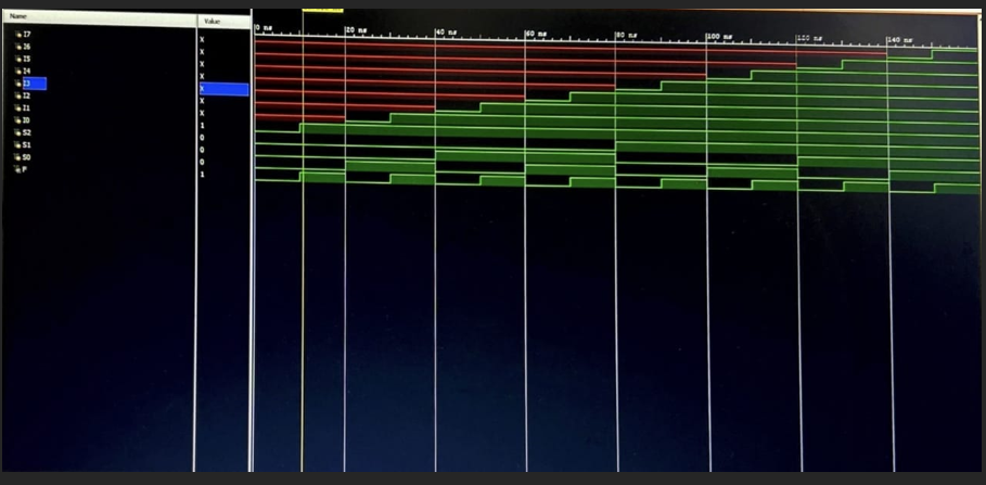
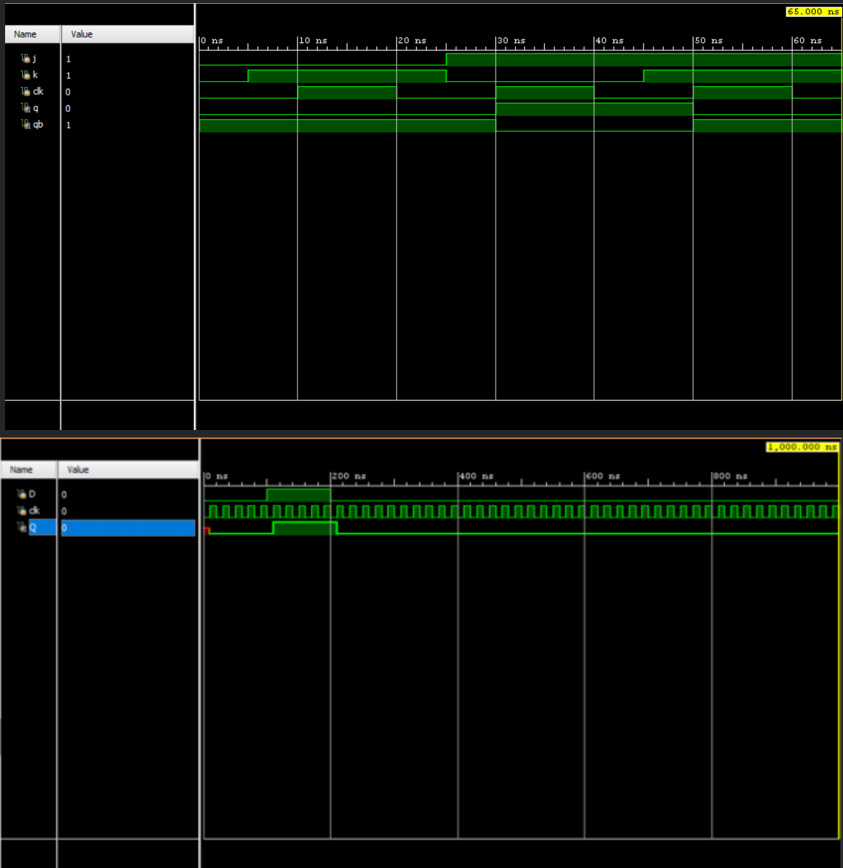
Testbench Simulation:
Experiment 6:(Design and simulation of modulo counter using Verilog behavioral modeling. Design modulo counter using JK flip-flops.)
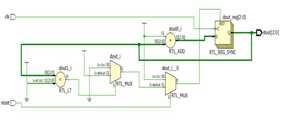
RTL Schematic:
Testbench Simulation:

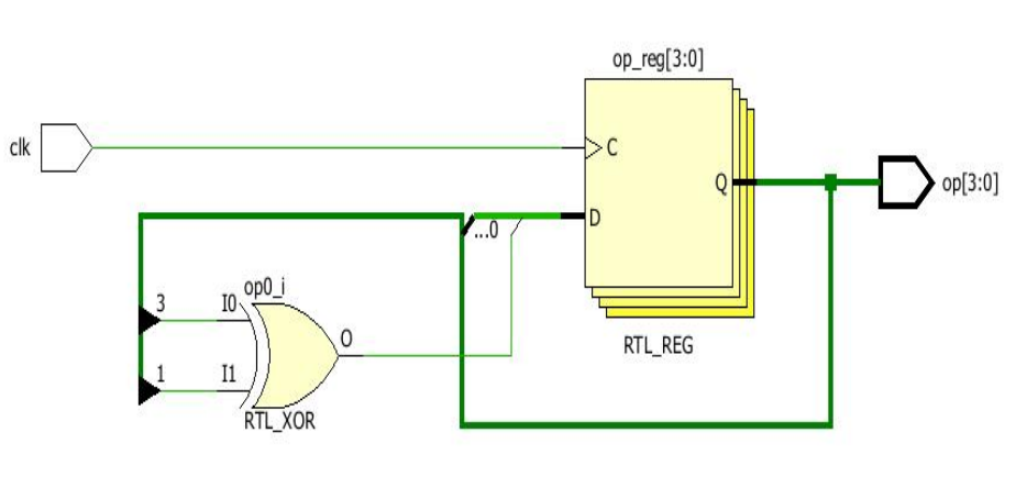
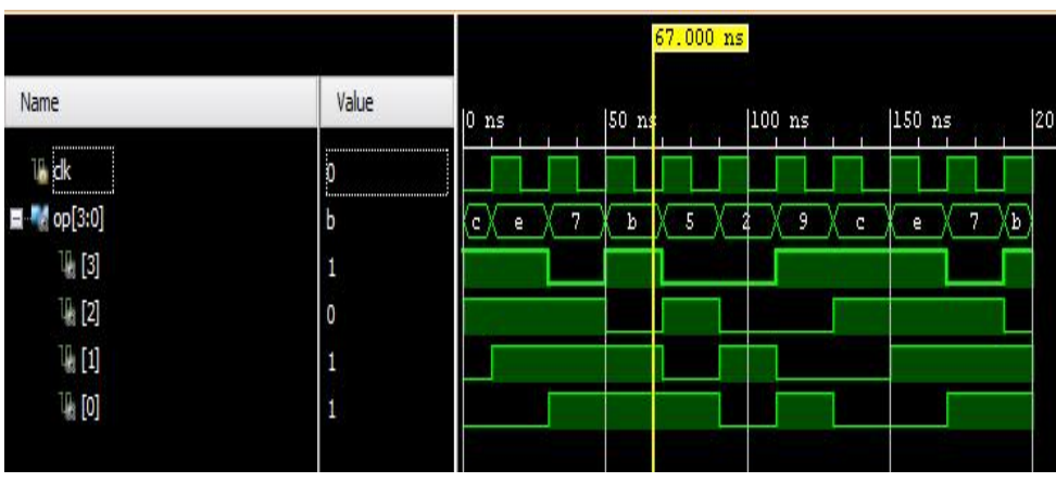
Experiment 7:(Design and simulation of a pseudo random sequence generator in Verilog. Implementation of pseudo random sequence generator using shift register)
RTL Schematic:
Testbench Simulation:
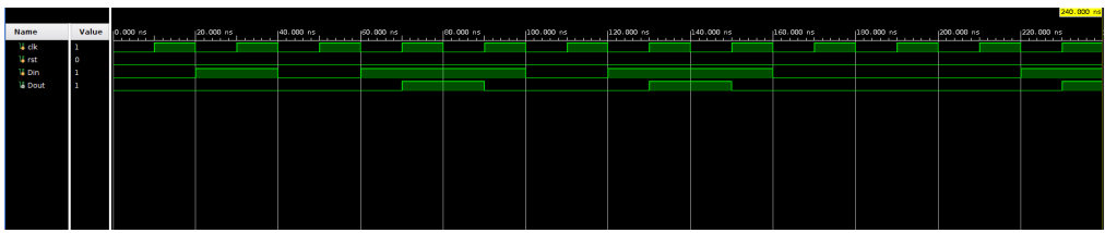
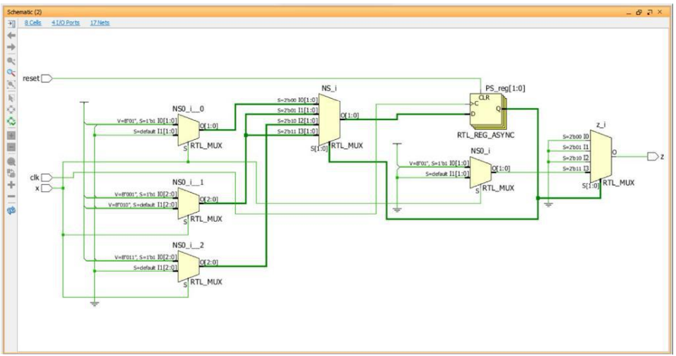
Experiment 8:(Design and simulation of a finite state machine in Verilog to detect a given sequence of bits)
RTL Schematic:
Testbench Simulation: